


 Contact Platform Support
 Help Center
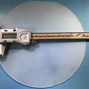
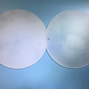
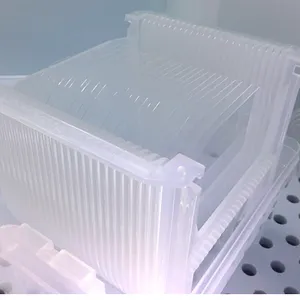
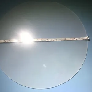
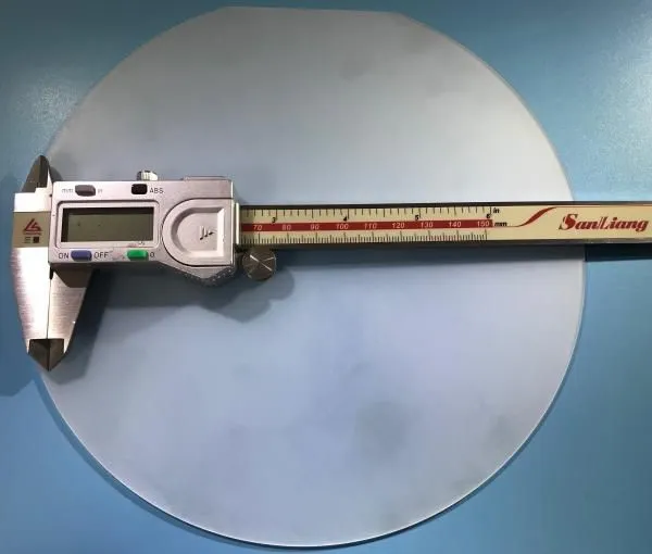
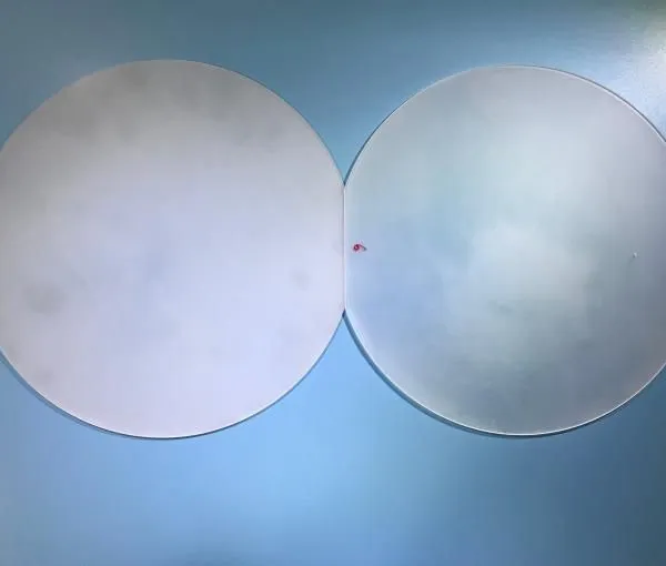
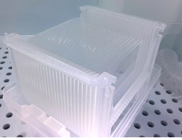
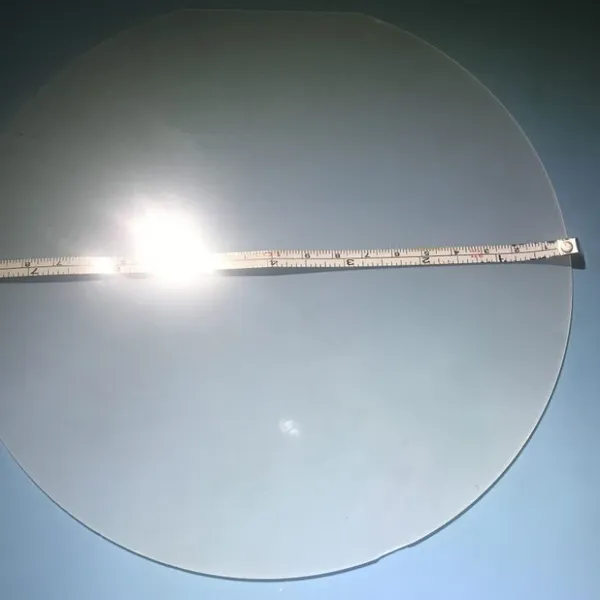
200mm 8inch Al2O3 Sapphire Optical Windows , Silicon Substrate SSP DSP 1.0mm C – Axis
Product Spotlights
Silicon Substrate



Related Products
-
 12inch C-aixs Al2O3 Sapphire Wafer Double Side PolishedNegotiableMOQ: 10 Blades
 -
ZnSe Window Zinc Selenide Optical WaferNegotiableMOQ: 10 Blades
-
ZnTe Crystal Substrate Orientation 110 10x10x0.5mm 10x10x1mmNegotiableMOQ: 10 Blades
-
High Purity Sapphire Crystal Watch Face Customized Size Polished SurfaceNegotiableMOQ: 10 Blades
-
UV&IR Calcium Fluoride (CaF2) WindowsNegotiableMOQ: 10 Blades
We can supplie 8inch/6inch/5inch/ 2inch /3inch 4inch /5inch C-axis/ a-axis/ r-axis/ m-axis 6″/6inch dia150mm C-plane Sapphire SSP/DSP wafers with 650um/1000um Thickness
Material:Sapphire Single CrystalOrientation:C-axisSurface:Ssp Or DspThickness:0.5mm Or CustomizedApplication:Led Or Optical GlassGrowth Method:KyHigh Light:sapphire wafer, sapphire material
About synthetic sapphire crystal
| GENERAL | |||
| Chemical Formula | Al2O3 | ||
| Crystal Stucture | Hexagonal System ((hk o 1) | ||
| Unit Cell Dimension | a=4.758 Å,Å c=12.991 Å, c:a=2.730 | ||
| PHYSICAL | |||
| Metric | English (Imperial) | ||
| Density | 3.98 g/cc | 0.144 lb/in3 | |
| Hardness | 1525 – 2000 Knoop, 9 mhos | 3700° F | |
| Melting Point | 2310 K (2040° C) | ||
| STRUCTURAL | |||
| Tensile Strength | 275 MPa to 400 MPa | 40,000 to 58,000 psi | |
| at 20° | 400 MPa | 58,000 psi (design min.) | |
| at 500° C | 275 MPa | 40,000 psi (design min.) | |
| at 1000° C | 355 MPa | 52,000 psi (design min.) | |
| Flexural Stength | 480 MPa to 895 MPa | 70,000 to 130,000 psi | |
| Compression Strength | 2.0 GPa (ultimate) | 300,000 psi (ultimate) |
Sapphire Properties
The Kyropoulos process (KY process) for sapphire crystal growth is currently used by many companies in China to produce sapphire for the electronics and optics industries.
High-purity, aluminum oxide is melted in a crucible at over 2100 degrees Celsius. Typically the crucible is made of tungsten or molybdenum. A precisely oriented seed crystal is dipped into the molten alumina. The seed crystal is slowly pulled upwards and may be rotated simultaneously. By precisely controlling the temperature gradients, rate of pulling and rate of temperature decrease, it is possible to produce a large, single-crystal, roughly cylindrical ingot from the melt.
After single crystal sapphire boules are grown, they are core-drilled into cylindrical rods, The rods are sliced up into the desired window thickness and finally polished to the desired surface finish.
Use as substrate for semiconducting circuits
Thin sapphire wafers were the first successful use of an insulating substrate upon which to deposit silicon to make the integrated circuits known as silicon on sapphire or “SOS”, Besides its excellent electrical insulating properties, sapphire has high thermal conductivity. CMOS chips on sapphire are especially useful for high-power radio-frequency (RF) applications such as those found in cellular telephones, public-safety band radios, and satellite communication systems.
Wafers of single-crystal sapphire are also used in the semiconductor industry as substrates for the growth of devices based on gallium nitride (GaN). The use of sapphire significantly reduces the cost, because it has about one-seventh the cost of germanium. Gallium nitride on sapphire is commonly used in blue light-emitting diodes (LEDs).
Used as a window material
Synthetic sapphire (sometimes referred to as sapphire glass) is commonly used as a window material, because it is both highly transparent to wavelengths of light between 150 nm (UV) and 5500 nm (IR) (the visible spectrum extends about 380 nm to 750 nm, and extraordinarily scratch-resistant. The key benefits of sapphire windows are:
* Very wide optical transmission band from UV to near-infrared
* Significantly stronger than other optical materials or glass windows
* Highly resistant to scratching and abrasion (9 on the Mohs scale of mineral hardness scale, the 3rd hardest natural substance next to moissanite and diamonds)
* Extremely high melting temperature (2030 °C)
CATALOGU & Stcok List
|
Standard wafer(customzied) 2 inch C-plane sapphire wafer SSP/DSP |
Special Cut |
Customized Size |
Patterned Sapphire Substrate (PSS) |
Specification for substrates
| Orientation | R-plane, C-plane, A-plane, M-plane or a specified orientation |
| Orientation Tolerance | ± 0.1° |
| Diameter | 2 inches, 3 inches, 4 inches, 5inch,6 inches, 8 inches or others |
| Diameter Tolerance | 0.1mm for 2 inches, 0.2mm for 3 inches, 0.3mm for 4 inches, 0.5mm for 6 inches |
| Thickness | 0.08mm,0.1mm,0.175mm,0.25mm, 0.33mm, 0.43mm, 0.65mm, 1mm or others; |
| Thickness Tolerance | 5μm |
| Primary Flat Length | 16.0±1.0mm for 2 inches, 22.0±1.0mm for 3 inches, 30.0±1.5mm for 4 inches, 47.5/50.0±2.0mm for 6 inches |
| Primary Flat Orientation | A-plane (1 1-2 0 ) ± 0.2°; C-plane (0 0-0 1 ) ± 0.2°, Projected C-Axis 45 +/- 2° |
| TTV | ≤7µm for 2 inches, ≤10µm for 3 inches, ≤15µm for 4 inches, ≤25µm for 6 inches |
| BOW | ≤7µm for 2 inches, ≤10µm for 3 inches, ≤15µm for 4 inches, ≤25µm for 6 inches |
| Front Surface | Epi-Polished (Ra |
| Back Surface | Fine ground (Ra=0.6μm~1.4μm) or Epi-polished |
| Packaging | Packaged in a class 100 clean room environment |

Send Inquiry to This Supplier


You May Also Like
-
Customized Size 8 Inch Sapphire Wafer SubstrateNegotiableMOQ: 25 Blades
-
Synthetic AL2O3 Sapphire Crystal Sapphire Glass Tube and PipeNegotiableMOQ: 10 Pieces
-
4Inch Prime Grade 4H-N 1.5mm SIC Silicon Carbide WaferNegotiableMOQ: 10 Blades
-
2-4inch N/P TYPE Semiconductor Substrate InAs Monocrystalline Crystal Substrates WafersNegotiableMOQ: 10 Blades
-
12 Inch SIC Substrate Silicon Carbide Prime Grade Diameter 300mm Large Size 4H-N Suitable for High Power Device Heat DissipationNegotiableMOQ: 25 Boxes
-
6″ (150mm) High Resistivity Float Zone Silicon WaferNegotiableMOQ: 25 Boxes
-
SOI Wafers Three Layer StructureNegotiableMOQ: 25 Boxes
-
12 Inch Sapphire Substrate Dia 300mm C Plane Quartz Wafers BF33NegotiableMOQ: 10 Blades
-
6 Inch N Type Polished Silicon Wafer DSP SiO2 Silicon Oxide WaferNegotiableMOQ: 10 Pieces
-
10*10*0.5 mm Semi P Grade 4H-N Semi SiC Chips Silicon Carbide WaferNegotiableMOQ: 10 Blades

