


 Contact Platform Support
 Help Center
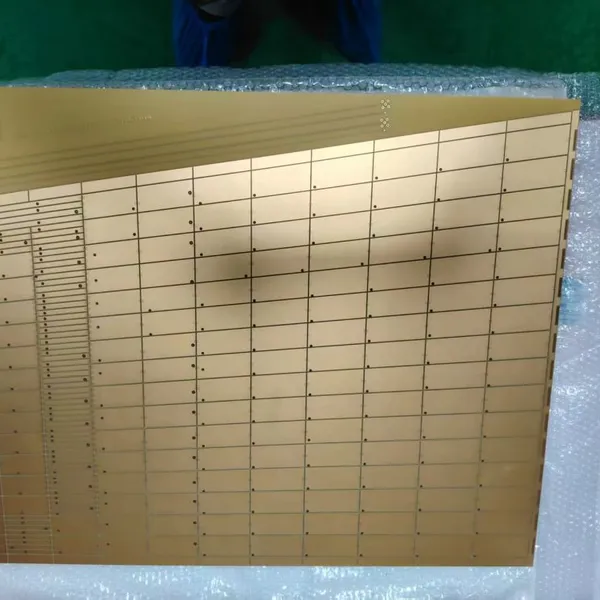
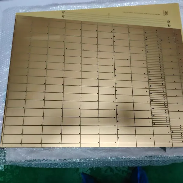
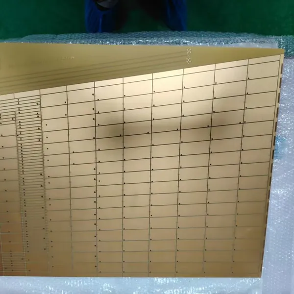
China Super Sheng, Ultra Large Size Multi-layer Whole Board Gold-plated Circuit Board PCB, Nuclear Product PCB
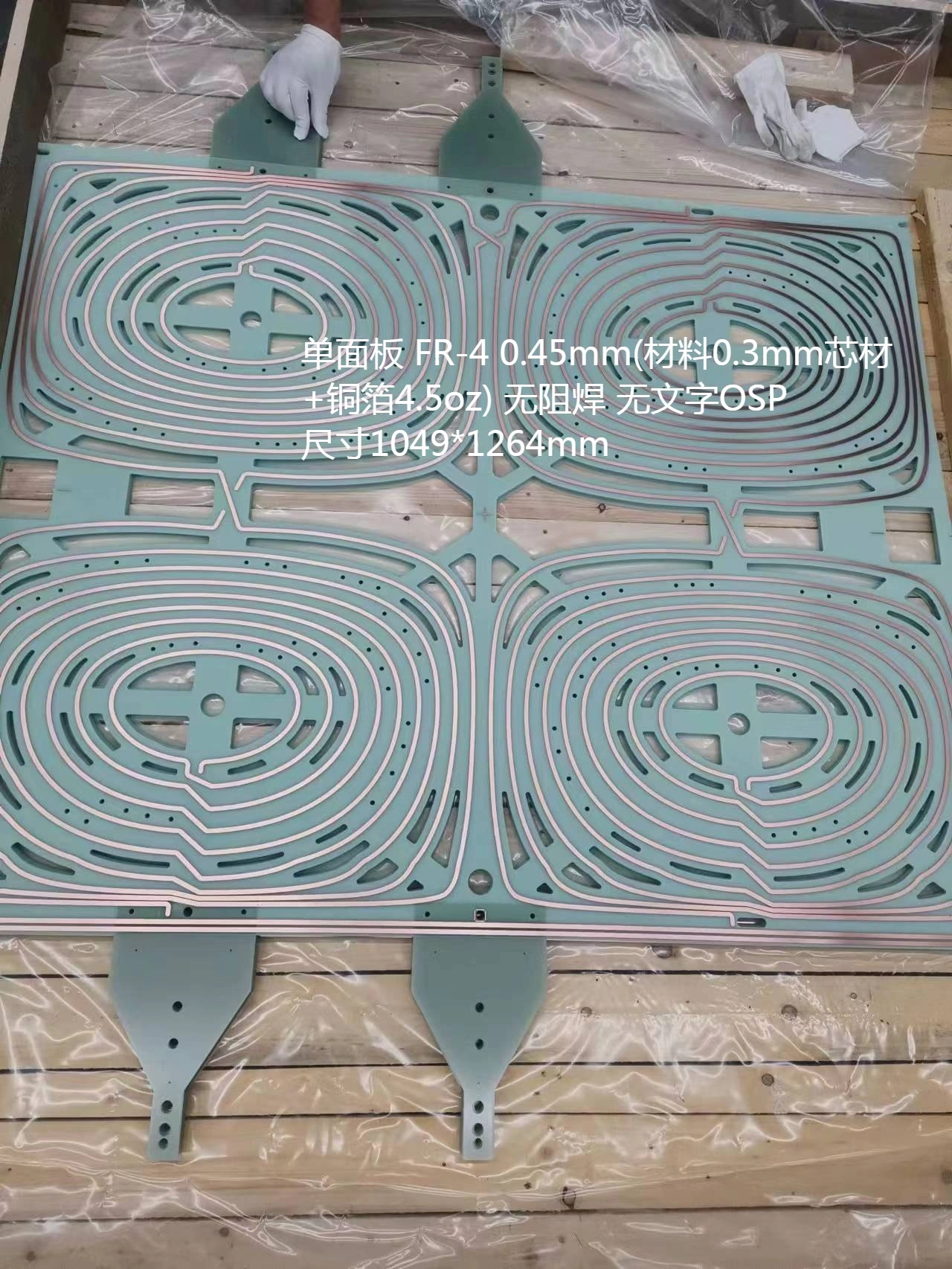


Product Spotlights




Related Products
-
 China Chaosheng Electronics | 1650 × 700mm Ultra Large Size Four Layer 3OZ Thick Copper Nickel Gold Circuit Board PCBNegotiableMOQ: 1 Blade
 -
China Chaosheng Electronics | Aerospace Grade Ultra Large Size 3OZ Thick Copper Four Layer Nickel Gold Printed Circuit BoardNegotiableMOQ: 1 Blade
-
China Chaosheng Electronics Automotive Products Multi Layer Flexible FPC Multi Layer Soft Hard Combination Flexible FPCNegotiableMOQ: 1 Blade
-
China Chaosheng Electronics' Large-scale Aviation, Large-scale Unmanned Aerial Vehicles, and Ultra Large PCBNegotiableMOQ: 1 Blade
-
16 Layer Ultra Large Size PCB,double-layer Ultra Large PCB,NegotiableMOQ: 5 Units
China Chaosheng Electronics | Introduction to seven layer HDI ultra large size, no solder mask, and whole board gold sinking PCB products
1、 Product Overview
This seven layer high-level HDI ultra large size circuit board is a customized high-end special PCB from China Chaosheng Electronics. It adopts a 7-layer stacked HDI blind buried hole stacking structure and is manufactured based on the company's ultra large size full process production line. The board surface completely eliminates solder mask ink coverage and undergoes chemical nickel deposition gold (ENIG) surface treatment. It meets the four core requirements of ultra large format carrying, high-density high-speed wiring, global bare copper thermal conductivity, stable welding and oxidation resistance, and is suitable for high-precision high-end equipment such as AI computing power equipment, large industrial vision, high-end medical testing, and large optical communication modules.
2、 Core technology and hardware advantages
1. Seven layer HDI high-density interconnect architecture
Adopting a standard 7-layer Build up HDI stack, combined with laser micro blind buried hole technology, the minimum laser aperture can reach 0.076mm, achieving short path interconnection between layers and reducing signal attenuation and crosstalk; Supporting ultra-fine 7/7mil fine circuits, capable of carrying high-density BGA and microchip layouts, with precise impedance control of ± 3%, meeting the high-speed differential signal transmission standard supplier network.
Symmetrical vacuum compression process, precise compensation for multi-layer compression expansion and contraction, to prevent warping and delamination explosion of high-rise boards;
Resin plug holes and electroplated filling holes in the tray, with uniform copper thickness on the hole walls, and no open circuit hazards during long-term high and low temperature cycling.
2. Exclusive production capacity for ultra large sizes (exclusive production capacity of Chaosheng)
Equipped with a 2600 × 1500mm large CNC drilling rig, a 2180 × 1200mm vacuum laminating machine, and a fully automatic large format LDI laser imaging equipment, the 7-layer HDI product supports a maximum of 1250 × 1150mm ultra large format, solving the pain points of large-scale multi-layer HDI that cannot be mass-produced, board deformation, and alignment deviation in the industry. A single board integrates multiple signals and power circuits, reducing the number of assembled boards and simplifying the assembly structure.
3. Full surface bare copper design without solder mask (special customized process)
The entire board does not print any solder mask green oil, and the copper foil lines, pads, and large areas of copper skin are completely exposed. Compared with conventional solder mask PCBs, it has unique advantages:
Global efficient heat dissipation: No ink insulation layer, copper surface directly contacts the heat sink/thermal medium, heat dissipation efficiency is increased by more than 60%, suitable for high-power and high heating modules, avoiding high temperature frequency reduction and device aging;
Welding and bonding without obstruction: no ink blocking welding, no risk of oil leakage, supports large-area mounting, gold wire bonding, multi-point low-temperature welding, greatly reducing the rate of virtual welding and welding defects;
Stable conductive contact: Bare copper is fully conductive, allowing for direct conductive grounding and multi-point spring contact, meeting equipment shielding and high current conduction design requirements;
Intuitive and convenient detection: The board surface is unobstructed by ink, and electrical and AOI appearance inspections can directly identify circuit defects, improving quality inspection efficiency.
4. Full coverage chemical gold deposition process for the entire board
The fully bare copper surface is uniformly treated with chemical nickel gold, with a nickel layer of 3-5 μ m as the base and a gold layer of 0.05-0.15 μ m covering the entire surface, without any leakage or thin gold areas
Ultimate antioxidant: Bare copper can be stored for a long time without oxidation or blackening under high temperature conditions, solving the problem of easy oxidation and scrap of bare copper in non resistance welding;
Wear resistant and plug resistant: The gold layer has high hardness, and it can withstand repeated contact and insertion and removal of tens of thousands of times without wearing or exposing copper;
Good welding consistency: uniform wetting performance across the entire area, no local differences in weldability, suitable for batch SMT automation production;
Adaptation to harsh environment: resistant to damp heat, cold and hot shock, meeting the long-term stable service requirements of industrial, medical and communication equipment Tiktok.
3、 Key technical parameters
Board structure: 7-layer HDI laminated blind buried hole board
Maximum finished size: 1250 × 1150mm
Minimum line width and spacing: 7mil/7mil
Minimum laser blind hole: 0.076mm
Surface technology: full surface solder mask, full area chemical deposition nickel gold (ENIG)
Impedance control: single ended 50 Ω/differential 100 Ω, tolerance ± 3%
Applicable substrate: High TG FR4/Low loss high-speed board can be selected as needed
Thickness range: 1.0-3.0mm, thickness tolerance ± 0.05mm
4、 Applicable application scenarios
AI large computing power server motherboard, industrial machine vision ultra large imaging module, high-end medical image detection equipment, large optical communication exchange backplane, rail transit control motherboard, large automation testing equipment, high-power intelligent detection industrial control board and other large-sized, high-density, high heat generating, multi-point welding/bonding high-end equipment.
5、 Chaosheng Electronics Supply Guarantee
We have our own large-size full process production line and stable batch production of 7-layer HDI non resistance welding sinking gold plates, without the need for outsourcing or cooperation, with controllable delivery time;
Base materials, copper foil, and gold plating solution should be locked in advance to prepare for the continuous price increase of raw materials and the shortage of supply. Spot prices should be locked and bulk production should be prioritized;
The entire process follows the IPC Class3 high reliability standard, with complete material reports, impedance testing, and reliability aging testing data to meet customer IATF16949 and system factory inspection requirements;
Support rapid prototyping and large-scale synchronous order acceptance, and can cooperate with customers to optimize stacking, heat dissipation, and wiring solutions, providing one-stop solutions to the manufacturing difficulties of large-sized high-level special PCBs.
6、 Purchase reminder (embedded in product introduction, not placed at the beginning or end)
The storage of bare copper immersion gold plates without resistance welding requires sealed vacuum packaging and storage with desiccants to avoid accelerated gold layer loss in humid environments;
In high-power application scenarios, copper thickness can be increased as needed (2-4 oz) to enhance high current carrying and thermal conductivity;
It is recommended to use customized fixtures and jigs for the assembly of oversized boards to prevent scratching of the gold layer during transportation and installation;
The drawings must fully indicate the requirements for full area solder mask, the standard for immersion thickness, and the impedance control range to avoid any deviation in process understanding.
7、 Summary of industry pain point solutions
There are generally three major shortcomings in similar products on the market: the difficulty of mass production of large-sized multi-layer HDI, the restriction of heat dissipation by solder mask layer, and the easy oxidation of bare copper without protection; China Super Sheng's seven layer HDI ultra large size solder mask PCB with gold deposition, relying on its own large format high-end equipment and mature special gold deposition technology, solves the four major industry problems of size limitation, insufficient heat dissipation, bare copper oxidation, and poor soldering in one go. It is the preferred solution for high-power, large high-end precision equipment circuit boards.
| FAQ | |||
| Serial Number | Question Point | Answer | |
| Q1 | Q: What information is required to make a PCB | CEGSATE: Gberber files for PCB production, product process instructions, such as material requirements, surface treatment requirements, finished product thickness requirements, PCB stack structure diagram for advanced products, copper thickness requirements for each layer, sample quantity requirements, batch order requirements, product application fields, and other related information are required | |
| Q2 | Q: What information does PCBA need to provide | CEGSATE: BOM report is required (including the brand, specifications, and model of the components), X and Y coordinate numbers of PCBA components, and processing requirements: Do we need to purchase the components on our behalf? Or customer supplied components? Do you need software burning? What is the required quantity? What is the monthly demand and other detailed information. | |
| Q3 | Question: Is my file secure? | CEGSATE: Your files are very secure, and we protect intellectual property rights for our clients throughout the entire process. All files provided by the customer will never be shared with any third party. | |
| Q4 | Q: What is the minimum order quantity? | CESGATE: We do not have a minimum order quantity for PO orders. We are able to handle small and large batches flexibly. | |
| Q5 | Q: What is your inspection method? How do you control the quality? | CESGATE: In order to ensure the quality of PCB, FPC, and PCBA products, we use flying pin testing for small batches, which is usually used for samples and small batches; The inner circuit undergoes 100% optical inspection through AOI, and we have online AOI automatic inspection for intermediate inspection. Batch finished products undergo 100% inspection through E-SET testing rack. The appearance is 100% inspected by fully automated finished product testing equipment and FQC. PCBA undergoes automatic optical inspection (AOI), 100% X-ray inspection of BGA parts, and first article inspection (FAI). PCBA products that require software burning must undergo 100% comprehensive testing on the finished product testing rack according to product functional requirements before they can be shipped. |
|
| Q6 | Q: What standard should PCB be shipped according to? |
WCESGATE: e accept and store according to the international IPC-6012 Level 2 standard. If there are special requirements for Level 3 standards in the quotation, we accept and store according to the international IPC-6012 Level 3 standardWe accept and store according to the international IPC-6012 Level 2 standard. If there are special requirements for Level 3 standards in the quotation, we accept and store according to the international IPC-6012 Level 3 standard |
|
| Q7 | Q: May I ask how you package and ship? | 1:PCBVacuum packaging+separated white paper+moisture-proof beads+cardboard box 2:PCBVacuum packaging+white paper insulation+moisture-proof beads+tin vacuum packaging+cardboard box 3:PCBSpecial size PCB, vacuum packaging+separated white paper+moisture-proof beads+wooden frame or plastic bag packaging+separated white paper+moisture-proof beads+wooden frame 4: PCBA anti-static packaging 5: PCBA anti-static film+vacuum box packaging+shelving |
|

Send Inquiry to This Supplier



You May Also Like
-
South Grid System Ultra Large Size Double-layer PCB,Apple Phone Ultra-thin Charging Head PCBNegotiableMOQ: 5 Units
-
2-layer Thick Copper Ultra Large Size Circuit Board PCB,Oversized and Large Hole PCBNegotiableMOQ: 5 Units
-
6 Extra Long Perforated PanelsPCB,Hole Board Circuit Board PCBNegotiableMOQ: 10 Units
-
2-layer Ultra Long Circuit Board PCB,Ultra Long Gong Hollow Board PCB,Multi Layer Ultra Long PCBNegotiableMOQ: 10 Units
-
4 Layers of Ultra Large Thin Circuit Board PCB,Large Sized Drone Circuit Board PCBNegotiableMOQ: 5 Units
-
16L High Frequency Mixed Pressure HDIPCB,Oversized PCBNegotiableMOQ: 10 Units
-
16 Layers, Second Order Ultra Large Size Circuit Board PCB,Multi Layer Ultra,large Size Circuit Board PCBNegotiableMOQ: 1 Unit
-
1 Layer Circuit Board PCB,Oversized and Large Hole PCBNegotiableMOQ: 1 Blade
-
1 Layer of Copper Surface Drilled Dense Hole Circuit Board PCB,CERN Dense Large Hole Large Scale PCBNegotiableMOQ: 1 Blade
-
1 Layer of Copper Surface Drilled Dense Hole Circuit Board PCB,Ultra Long Gong Hollow Board PCBNegotiableMOQ: 1 Blade


